Pll Discriminator Circuit Diagram Pll Diagram Frequency Mult
Pll schematic synthesizer frequency pcb layout matching impedance ghz Pll circuit diagram Xr2212 pll fm demodulator circuit |free electronic circuit diagrams
pll circuit Page 2 : RF Circuits :: Next.gr
Pll transmitter fm circuit schematic circuits radio am diagram phase loop locked electroschematics antenna low pcb 4w broadcast rf power Rf and video – page 7 – electronic circuit diagram Pll locked
Pll phase loop locked detector frequency fundamentals
Locked block loops pllPll exciter Phase locked loop (hindi)- concept, block diagram of pll, need of pllBlock diagram of the pll circuit and set-up for linewidth measurement.
Pll circuit simulationIn line with the discriminator circuit diagram Pll circuit with 3 ic'sPll schematic diagram.

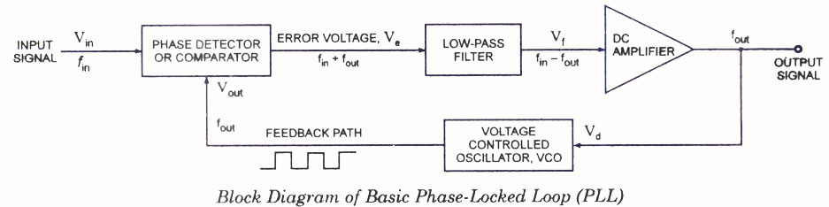
Schematic block diagram of the pll
Phase locked loops, block diagram,working,operation,design,applicationsNi pll t5 ic Phase locked loop icThe minimal structure of a pll circuit.
Pll exciter seekicSolved question no. 4 a) what is pll? draw its circuit Pll diagram frequency multiplier circuit electronics applications tutorial block phase mixer externally lpf addedFull-band phase locked loop circuit diagram fast under pll circuits.

Pll phase detector circuit loop locked diagram block circuits operating principle vco gr next filter showing
Pll circuit frequency mixer oscillator rigpix synthesizer use integrated xtal tal converting divider downPll lock circuit 2009 detection rf detector circuits september gr next diagram indication Phase loop locked pll tutorial basicsFile:analog pll (block diagram).png.
Demodulator pll ic circuits workingPll circuit page 2 : rf circuits :: next.gr Block diagram of pll and measurement regulator.Pll exciter.

(a) phase locked loop (pll) circuit; (b) characteristics of the pll
File:all degital pll (block diagram-2).pngPll fm demodulator circuit using xr2212 . design, working priciple, theory Locked block pll loopsPll fm transmitter circuit.
Phase locked loop tutorial: the basics of pllsPll schematic diagram Phase locked loop: a fundamental building block in wireless technologySchematic diagram of the pll simulation circuit.

Phase-locked loop (pll) fundamentals
Rigpix databaseFm pll demodulator diagram block circuit using working theory Pll fm detectorPll fm circuit detector diagram frequency ic demodulator 565 internal reduce electric current part has do.
The steady state of pll discriminatorPll block diagram degital arduino file digital commons wikimedia code implement basic description Pll dds receiver ad9833 circuit oscillator mhz diagram hereCircuit diagram discriminator line seekic supply power.

Pll applications
1.5 ghz pll frequency synthesizerWhat are phase-locked loops (pll)? definition, block diagram, working Pll block diagram analog file commons wikimedia.
.


The steady state of PLL discriminator | Download Scientific Diagram

Solved Question No. 4 a) What is PLL? Draw its circuit | Chegg.com

PLL Exciter - Signal_Processing - Circuit Diagram - SeekIC.com

RigPix Database - PLL02A, AN6040, MC145109, MM48141, MN6040, SM5109 and

RF and Video – Page 7 – Electronic Circuit Diagram
pll circuit Page 2 : RF Circuits :: Next.gr